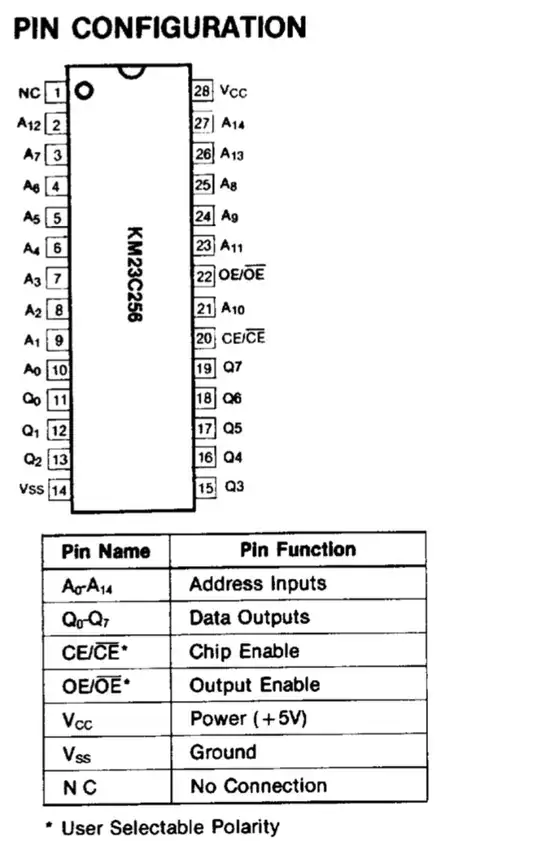
I am reverse-engineering a late-'80s IBM Wheelwriter typewriter, which runs off of an Intel 8088. It has a ROM chip, specifically: https://www.datasheets360.com/pdf/1277907997291200345?xrefPartId=1277907997291200345&alternatePartManufacturerId=0
in a socket that holds the X86 code, and I'd like to emulate that chip by responding to memory requests via my Raspberry Pi, through the GPIO pins.
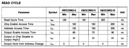
I am concerned that I won't be able to read the 14 address pins and respond on the 8 data pins fast enough. Here is the timing data:
Before I go and build the circuit, is this something that will be doable? What other things should I measure? Based on my logic analyzer readings, it looks like the pulse width coming from the 8088 is about 120ns.

