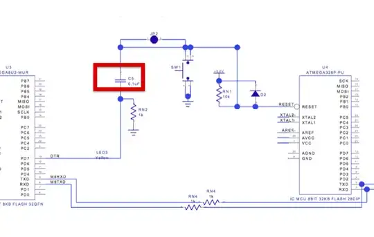
The Atmel datasheet, page 305, Section 29.5 "System and Reset Characteristics" provides some useful information for the reset pulse. It says that the worst-case minimum pulse width is \$2.5\:\mu\textrm{s}\$. It then goes on to say that the ramp rate has to be contained between two boundaries; no faster than \$10\:\frac{\textrm{kV}}{\textrm{s}}\$, but also no slower than \$10\:\frac{\textrm{V}}{\textrm{s}}\$. So there are some restrictions that should be managed by any reset system.
There are some nice reset circuit ICs available which provide a manual reset input as well as a control line. I'd probably use one of those about a circuit I cared about. Okay. Actually, I'd make my own out of a PIC10LF320 in a SOT-23-6, which also includes a brown-out circuit of its own, which I'd probably also re-purpose, as well.
But let's look at this circuit. DTR is normally held HIGH (I believe) and is pulled LOW in order to initiate a reset. Assuming that the two MCUs are running on different power rails (or the same, doesn't matter), \$C_5\$ is charged up to the difference between the ATmega328's rail (via \$RN_1\$ and the DTR output line's HIGH value.) If there is no difference, the voltage will be nearly zero. But if the rails are different, then there will be a small voltage across \$C_5\$ that represents this difference.
When DTR is pulled LOW, that end of \$C_5\$ is also pulled down to that voltage (close to ground.) For the first moments, this also means that the other side of \$C_5\$ is similarly pulled downwards, too. If there was some voltage rail difference, then that's the voltage that appears at the reset pin of the ATmega328. Depending on the voltage differences between the MCUs and the reset pin requirements of the ATmega328, this could be a problem. The datasheet says that it may be required to be as low as \$600\:\textrm{mV}\$, though the typical only requires to be pulled down to \$1.3\:\textrm{V}\$. But if no difference in the rails, then hopefully near-ground appears at the reset pin of the ATmega328. I'm going to assume there is no difference, here, so that we at least have a good chance it works okay.
Now, as soon as \$C_5\$ is yanked down by DTR, \$C_5\$ begins charging up through \$RN_1\$, starting at a rate of about \$500\:\mu\textrm{A}\$. The time constant is \$1\:\textrm{ms}\$. So the voltage will rise rapidly. Assume that we only just barely achieved the required \$600\:\textrm{mV}\$ at the start (the capacitor held a slight charge.) Then we'd cross over the minimum rising threshold of \$1.1\:\textrm{V}\$ within about \$100\:\mu\textrm{s}\$. This is well more than long enough for the earlier mentioned minimum reset pulse width of \$2.5\:\mu\textrm{s}\$. So the spec is met here.
Now, let's go the other direction. Let's say that now DTR is held LOW for a long enough time that it charges up to about \$5\:\textrm{V}\$ through \$RN_1\$. Now, DTR is driven HIGH. What happens? Well, the other side of \$C_5\$ will now be at about \$10\:\textrm{V}\$ (the \$5\:\textrm{V}\$ charge on \$C_5\$ added to the DTR HIGH voltage value.) This is rapidly discharged, safely, via \$D_2\$. That's why \$D_2\$ was added. Otherwise, this voltage would be presented to the RESET pin of the ATmega328 and would have to be discharged via any internal protection diodes present there (which may themselves have additional specifications that must be met.)
What's interesting here is that the RESET pin in particular is called out in the datasheet on page 299. It says that it can support up to \$13\:\textrm{V}\$ worst case. So, technically, that might mean that \$D_2\$ isn't necessary to avoid driving protection diodes in the CPU. But it is still a good idea for an entirely different reason. This is to discharge \$C_5\$ rapidly (it would be very slow, via \$RN_1\$), so that it can be used for another reset very soon after being used.
Note on the reset pin:
As Majenko added in a comment, there is a high voltage programming mode for Atmel devices like this. I frankly don't fully apprehend it, as I haven't read a datasheet on the topic. But I did find out from an Atmel video that the PC6/RESET line, which normally acts like a /RESET line, can be changed into operating like a general purpose I/O port by changing the RSTDISBL fuse, which makes the general I/O function available. The bad thing about that is that the ISP programming mode NEEDS the /RESET line to do its job. So you can't program the device anymore, if you set up that fuse. This then forces you to use the parallel programming mode that is entered using the high voltage programming mode. I would guess that entering this mode uses the /RESET pin again, but this time places a high voltage on it that is detected in order to put the device into its parallel programming mode instead of the ISP programming mode.
I can't readily find a specific programming document on the details of using this mode to program their devices. Microchip publishes them. But it appears, cursory examination only, that Atmel does not. They document how to use the mode with their tools, such as the STK500 (which I have.) But not how to design your own tool. I'm guessing, for now, that this is a matter of non-disclosure for Atmel. And given that they have it available for so many different devices, I can see why they might want to avoid having to support it.
The details on this pin are starting to get complicated-sounding. But pins cost money and silicon is cheap. So Atmel, like other companies, try to come up with methods to use their scarce pins to provide as much versatility as they can to sell devices.
That's it.
